
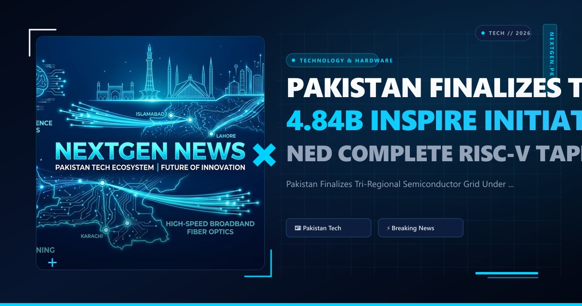
The Ministry of IT and Telecom has finalized Pakistan’s national tri-regional Semiconductor Education & Research Clusters (SERCs) under the Rs 4.844 billion INSPIRE program, anchoring domestic RISC-V System-on-Chip design, open-source silicon tape-outs, and cloud EDA infrastructure across Islamabad, Lahore, and Karachi.
In a transformative milestone for Pakistan’s hardware engineering ecosystem, the Ministry of Information Technology and Telecommunication (MoITT) has officially formalized the operational network of the INSPIRE (Initiative to Nurture Semiconductor Professionals for Industry, Research, and Education) program. Supported by a government budget allocation of PKR 4.844 billion, the national project establishes three interconnected Semiconductor Education & Research Clusters (SERCs) across Islamabad, Lahore, and Karachi.
The formal induction of Karachi’s NED University of Engineering and Technology as the South Region Lead—joining the National University of Sciences and Technology (NUST) in the North and the University of Engineering and Technology (UET) Lahore / ESUPAK in the Central Region—completes Pakistan’s first end-to-end national grid dedicated to fabless integrated circuit (IC) design, verification, and silicon prototyping.
Strategic Imperative: The Fabless Advantage
While establishing silicon wafer fabrication plants (foundries) demands tens of billions of dollars in capital expenditure, the global semiconductor value chain derives over 50% of total industry profit from front-end fabless design, intellectual property (IP) cores, and verification.
The INSPIRE initiative strategically channels state capital and academic labs exclusively into fabless chip architecture, leveraging the open-source RISC-V Instruction Set Architecture (ISA) to bypass costly proprietary licensing fees while building microprocessors tailored for edge AI, IoT sensing, defense avionics, and cryptographic hardware.
Regional Cluster Breakdown & Technical Mandates
The three SERC clusters operate on specialized, non-overlapping technological tracks to maximize domestic engineering bandwidth and streamline access to international multi-project wafer (MPW) foundry runs:
1. North Cluster: NUST (Islamabad) — Edge AI & High-Reliability ASICs
The NUST Chip Design Centre (NCDC) spearheads advanced logic design and compute accelerators. Key areas of focus include:
2. Central Cluster: UET Lahore / ESUPAK — Embedded SoCs & Open Silicon
Building upon the milestone launch of the Lahore Semiconductor Design and R&D Hub, UET Lahore’s Microelectronics Lab leads the open-source silicon vertical:
3. South Cluster: NED University (Karachi) — Post-Quantum Cryptography & Automotive Silicon
Operating from Pakistan’s commercial and maritime center, NED University’s Semiconductor Research Facility anchors:
Human Capital Target: 7,200 IC Engineers by 2030
The core bottleneck in the global semiconductor landscape remains the acute shortage of physical design and verification engineers. The PKR 4.844B INSPIRE program enforces aggressive capacity-building KPIs:
Through specialized Upskilling Training Programs (USTPs), mid-career electrical, electronic, and computer system engineers will undergo intensive 6-month residencies in SystemVerilog, UVM (Universal Verification Methodology), and physical place-and-route (P&R).
The Cloud EDA Infrastructure Bottleneck
Modern semiconductor design is fundamentally a high-performance computing (HPC) software problem. Running full-chip functional simulations, Monte Carlo transistor variations, parasitics extraction (PEX), and Design Rule Checks (DRC) on complex 28nm and 16nm nodes generates massive parallel compute demands.
To prevent proprietary Register-Transfer Level (RTL) IP leaks and comply with national strategic export controls, R&D labs and startup clusters cannot rely on unsecured third-party offshore shared instances.
Engineering teams running heavy EDA simulation batches, hardware compilation pipelines, and continuous regression suites require dedicated computing environments. Nextgen Hosting delivers sovereign, high-throughput compute infrastructure tailored for deep-tech workloads:
Integration with the Global Fabless Supply Chain
The INSPIRE roadmap connects domestic university tape-outs directly to global pure-play foundries—including TSMC (Taiwan), GlobalFoundries (Singapore/US), and SkyWater (US)—through aggregated Multi-Project Wafer (MPW) shuttle programs supported by EuroPractice and CMC Microsystems.
By coupling silicon-proven RTL designs with the PKR 5 billion Ignite Deep Tech Commercialization Program and the national Billion-Dollar AI Digital Stack Vision, Pakistan is transforming its IT export base from low-margin outsourced software services into high-value, defensible hardware intellectual property.
The completion of the tri-regional INSPIRE grid marks the definitive transition of Pakistan’s engineering sector from passive consumers of foreign technology into active architects of sovereign microelectronics.
🛠️ Related Technical Architecture Guides
- Enterprise Headless Browser Automation & Web Scraping on Cloud VPS: The Zero-Detection Architecture Guide – Enterprise implementation details and deployment guide.
- Diagnosing and Resolving Complex MariaDB Database Latency in WordPress on cPanel – Enterprise implementation details and deployment guide.